
Check the revision of the board because the pins of the GPU might be different. This guide is for GPU 315-5700 and 315-5660
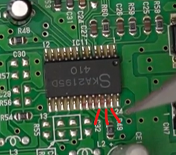
Lift the pins in the video encoder. First check that pins 21, 22 and 23 have continuity with the top 3 pins of the DIN connector. The lift those pins using an iron and xacto knife or tweezers
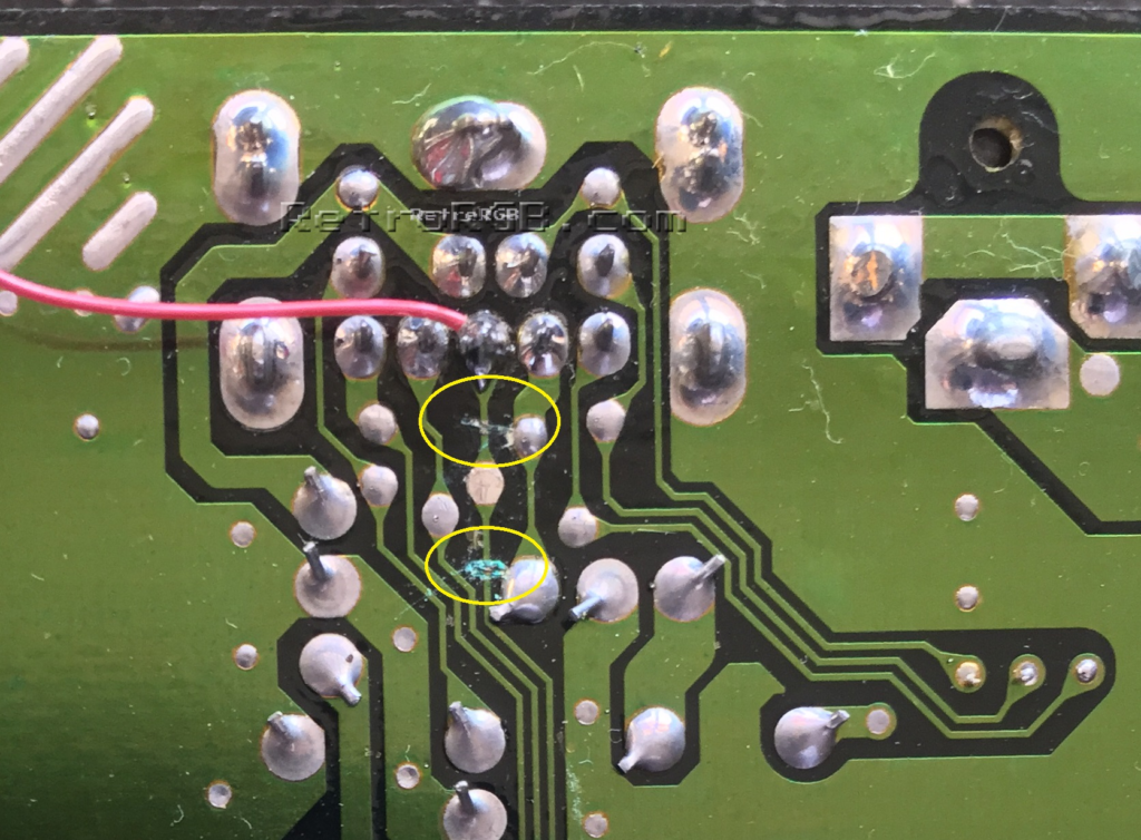
Cut traces around the csync point
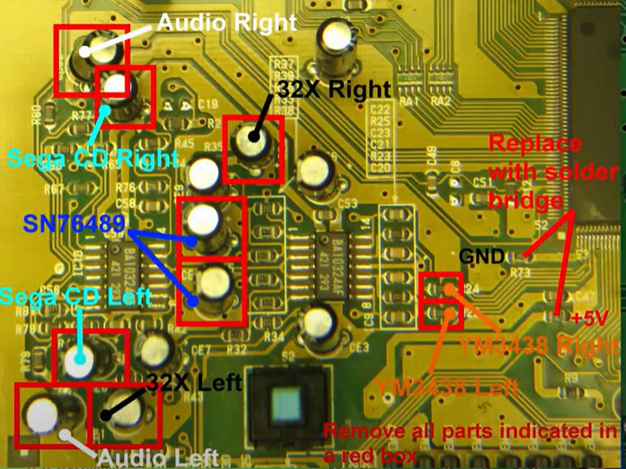
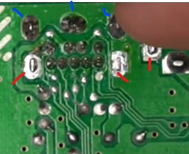
Remove the capacitors that will be used later for audio in the bypass board. For V1.8 are the ones below (all the ones with a red squate around them). For other boards might be different ones
Also remove the resistors R24 and R22, as well as R73 and R72, and replace these last two with a bridge
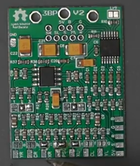
Next up, prepare the triple bypass board by looking at the back of the board and bridging the right pads. In the case of a v1.8, that’s pad marked as 2, then the c pads, the right 2 pads of the d pad group, and the e pads.
Also no need to worry about the resistors that might have come with the modkit because that’s only for version Va2 and Va4
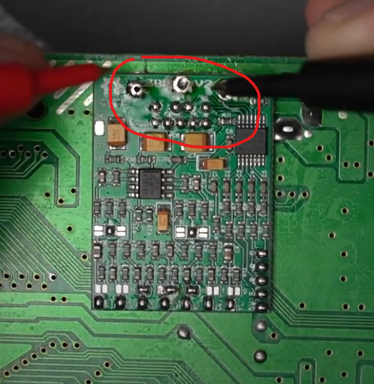
Next prepare the back of the DIN connector to make sure the triple bypass board goes in fully. That means remove the solder from the ones marked in red below and cut the pins with a flush cutter, and then for the ones marked in blue, remove some solder so that the pins go through completely through the board. I would make sure that the pins are still connected to the pads even if its flatter
Solder the board to the DIN pins. Make sure there is no bridges under the board. No adjacent pin should have continuity
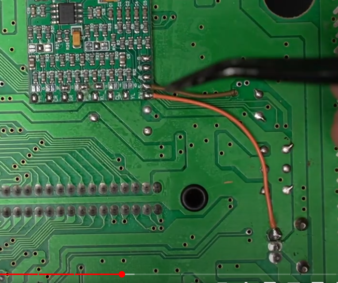
Next wire the 5V and the Sync line. The former goes to the “out” of the voltage regulator, and the sync line to the end of the trace we cut for csync. The sync point is connected to a via. To ensure best soldering, push the wire through the via a solder on the other side. The pads around the vias are masked, and you need to scrape the mas. However it is still difficult for solder to adhere, so scraping a bit of the trace that goes from that via and soldering to that works better.
Next are the YR and YL points on the audio. These go to the rightmost pad of the two resistors we removed earlier and which we didn’t bridge (the pads closer to the main chip). After soldering one end to the resistor pads, run the two wires towards the power connector, and push them through the hole near the connector to get to the bottom of board. Solder to YL and YR points.
For the rest of the 5 points, prepare a strand of 5 cables and fold is as per the picture below. Solder the points in the board first, making sure the cables are of the right length, then fold it and cut all of them to length before stripping and solder one by one. Note that they are being soldered to holes from caps we removed before, so there is only a pad on the back of the board. So even if its a good idea to push the wires through the holes before soldering, the soldering part is only in the back.
Reference material:
- RetroRGB: https://www.retrorgb.com/genesis2rgbbypass.html
- Youtube: https://www.youtube.com/watch?v=DrWRxkWPVwE